PCB Layers and Stackups: Engineering from Design Desk to Assembly Line
How layer count, dielectric physics, thermo-mechanical symmetry, and material selection dictate high-speed signal integrity, PDN impedance, and surface-mount reflow yield.
Layer count is one of the earliest decisions in any PCB program, and it is among the most expensive to get wrong. It establishes the impedance limits, the return-path geometry, how well the power distribution network (PDN) performs, the EMC compliance margin, the BGA escape capability, and how well the finished board survives surface-mount assembly. Changing layer count after routing begins invariably forces a costly and time-consuming layout re-spin.
Yet layer count is fundamentally only an integer. What dictates how a circuit assembly behaves in real-world operation is the stackup architecture: the ordering of signal and reference planes, dielectric thicknesses, resin content, copper weights, and thermo-mechanical balance. A poorly planned 8-layer stackup can easily perform worse in radiated emissions and assembly yield than a disciplined 4-layer design.
This engineering guide bridges the gap between EDA layout physics, bare-board fabrication constraints, and surface-mount production realities. Covering architectures from 2 to 16+ layers and HDI build-ups, we examine the underlying electromagnetic physics, provide practical stackup recipes, and detail exactly what each design decision triggers when the board enters the surface-mount reflow oven.
1. Introduction and Layer Count Quick Selector
Layer count should always be the analytical output of four distinct evaluations: BGA escape routing, high-speed interface inventory, PDN target impedance, and regulatory EMC limits. It must never be chosen based on intuition or legacy habits.
The quick selector table below provides an industry-proven baseline for determining your starting layer count before detailed routing begins. Every design should subsequently be validated against fabricator stackup sheets and assembly thermal profiles.
| Target System Architecture | Starting Layers | Recommended Stackup Recipe | Key Design Driver |
|---|---|---|---|
| Power supplies, LED drivers, simple analog, edge rates > 5-10 ns | 1-2 Layers | Solid bottom ground pour; CPWG for controlled impedance | Lowest bare-board cost; low di/dt loops |
| MCUs, USB 2.0 HS, 10/100 Ethernet, switching regulators, Class B EMC | 4 Layers | S-G-P-S (standard) or G-S-S-G (EMC critical shielded) | Direct GND referencing on outer signals |
| 0.8 mm BGAs, DDR3L/LPDDR, multi-rail PMICs, industrial & automotive | 6 Layers | S-G-S-P-G-S with symmetric core/prepreg dielectrics | BGA escape and balanced thermal symmetry |
| DDR4/DDR5, high-density FPGAs, PCIe Gen3/4, large application processors | 8-10 Layers | S-G-S-G-P-S-G-S (stripline routing pairs) | Tightly coupled PWR/GND and GND-shielded traces |
| 1,000+ ball BGAs, 25-112 Gbps PAM4 SerDes, sub-mOhm PDN, backplanes | 12-16+ / HDI | Multiple GND-referenced striplines; laser microvias (1+N+1 to ELIC) | Sub-0.65 mm ball pitch and ultra-low via stubs |
At Shematic, automated DFM and BOM analysis completes in under 60 seconds, followed by comprehensive engineering review in under 2 hours. Engaging early on stackup geometry eliminates trace width re-spins and assembly warpage before layout begins.
2. Construction Fundamentals: Cores, Prepregs, and Base Materials
Multilayer boards are constructed from three core elements: fully cured (C-stage) double-sided copper-clad cores, partially cured (B-stage) prepreg bonding sheets, and electrodeposited (ED) outer copper foils.
When heated and compressed during lamination, the prepreg resin liquefies, flows into the etched spaces of the adjacent copper layers, and cures completely into a rigid dielectric. Because resin flows into void spaces, the final pressed thickness of any prepreg sheet depends directly on the copper density of adjacent layers. A prepreg between a signal layer with 20% copper coverage and a solid plane with 95% copper will press significantly thinner than its nominal catalog thickness. Using CAD default values instead of the fabricator's pressed thickness calculation is one of the leading causes of impedance failure.
Furthermore, high-speed and lead-free manufacturing demands precise base material selection. Standard FR-4 with a glass transition temperature (Tg) of 130-140 deg C risks barrel cracking and delamination when subjected to repeated lead-free peak reflow temperatures of 245-260 deg C. For multilayer builds (6+ layers or boards over 1.6 mm), specifying high-Tg (Tg >= 170 deg C) and high-decomposition (Td >= 340 deg C) laminates is mandatory.
| Prepreg Glass Style | Approx. Pressed Thickness | Resin Content | Engineering Notes & Application |
|---|---|---|---|
| 106 | 0.04 - 0.05 mm | 70 - 75% | Thin, resin-rich; high Dk variation; fine-line HDI outer layers |
| 1080 | 0.06 - 0.075 mm | 62 - 68% | Standard choice for thin microstrip dielectrics on 6/8-layer builds |
| 2116 | 0.10 - 0.12 mm | 52 - 56% | Balanced general-purpose prepreg; good fill performance |
| 1652 | 0.13 - 0.14 mm | 48 - 52% | Thicker dielectric gap; reduces ply count in wide spacing |
| 7628 | 0.18 - 0.20 mm | 42 - 46% | Heavy coarse weave, economical; avoid under multi-Gbps differential pairs |
| 1035 / 1078 / 3313 | 0.07 - 0.10 mm | 50 - 60% | Spread flat glass; eliminates fiber-weave intra-pair timing skew |
3. Why Layer Counts Are Even: Thermo-Mechanical Balance
While odd layer counts (such as 3, 5, or 7 layers) are theoretically possible, they are practically never used in production electronics. The reasons are mechanical, thermal, and economic.
First, raw laminate cores are manufactured with copper clad on both sides. Fabricating a 5-layer board requires stripping copper completely from one side of a core, meaning you pay for copper foil that is instantly etched away as chemical scrap. A 5-layer board costs virtually the same as a 6-layer board.
Second, and far more critically, odd layer counts disrupt thermo-mechanical symmetry. Copper has a coefficient of thermal expansion (CTE) of approximately 17 ppm/deg C, whereas FR-4 expands at 13-17 ppm/deg C in the X-Y plane and up to 250-300 ppm/deg C in the Z-axis above Tg. When copper foil weights, dielectric heights, or glass styles are unbalanced about the board's physical centerline, unequal contraction stresses build up during lamination cool-down.
While the board may appear flat at room temperature, it warps aggressively when heated to 245-260 deg C during lead-free reflow. Under IPC-6012, maximum allowable bow and twist for surface-mount assemblies is 0.75% (representing 1.875 mm deflection on a 250 mm board). Dynamic reflow warpage easily exceeds this threshold on asymmetric builds, pulling BGA corner solder balls away from paste deposits and creating non-wet open or head-in-pillow joints.
1. Mirror layer order, dielectric thicknesses, and prepreg glass styles about the center. 2. Mirror finished copper weights (an L2 of 1 oz requires an L(N-1) of 1 oz). 3. Balance residual copper density across opposing layers using non-functional copper thieving on sparse signal layers.
4. Key Electrical Relationships: Impedance, Delay, and Return Paths
Controlled impedance is governed by the trace geometry, copper thickness, and dielectric distance to the nearest reference plane. Traditional closed-form IPC-2141 formulas provide useful intuition, but they lose accuracy on thin modern dielectrics where trace thickness represents a large fraction of dielectric height (t/h >= 0.3). Production trace widths must always be computed using 2D boundary-element field solvers incorporating solder mask effects.
Propagation delay in standard FR-4 (dielectric constant Er approx 4.0) is roughly 6.7 ps/mm (170 ps/inch) for stripline, while surface microstrip runs faster at 5.6-5.9 ps/mm due to fringing fields in air. A trace acts as a transmission line whenever its electrical length exceeds roughly one-sixth of the signal rise time: Lcrit approx tr / (6 x tpd). With modern sub-nanosecond switching edges (tr = 100 ps), any trace longer than 2.5 mm behaves as a transmission line requiring controlled impedance.
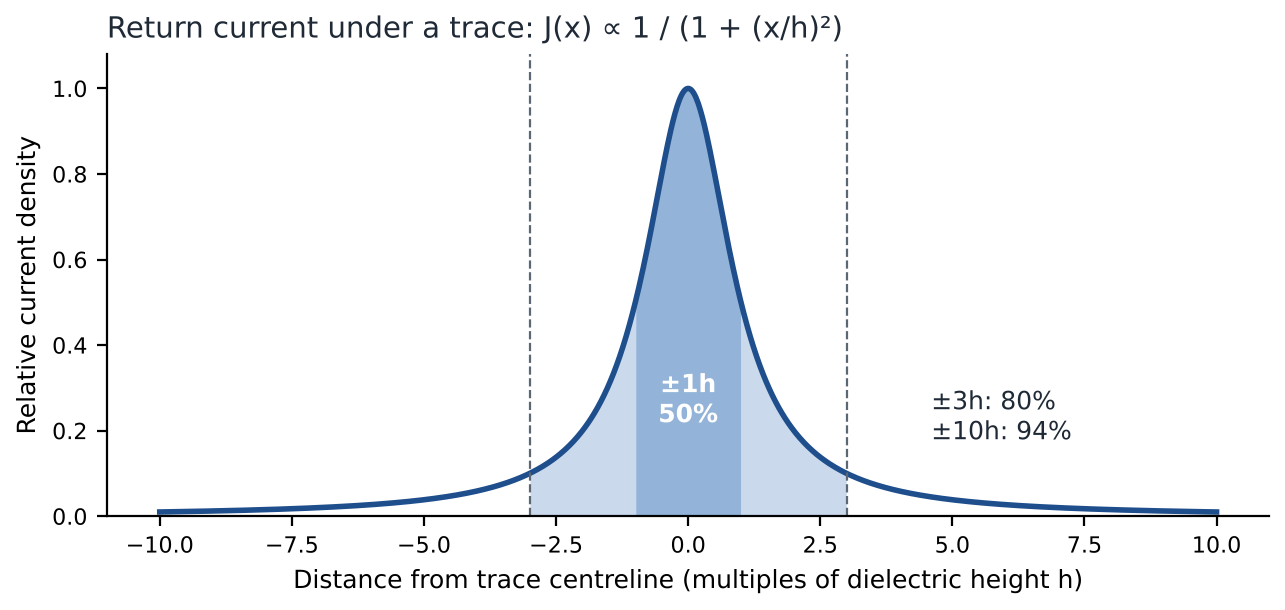
Crucially, high-frequency return currents do not take the path of least resistance; they follow the path of least inductance, concentrating in the reference plane directly underneath the signal trace. As shown in the field distribution below, approximately 50% of return current flows within +/- 1h of trace centerline, and 94% flows within +/- 10h. Any split or cutout in the reference plane forces return current around the obstacle, creating an expansive loop antenna that radiates electromagnetic interference and causes common-mode coupling.
| Dielectric Height (h) | IPC-2141 Trace Width | 2D Field Solver Trace Width | Practical Routing Assessment |
|---|---|---|---|
| 1.50 mm (2-layer board) | approx 2.80 mm | approx 2.90 mm (114 mil) | Impractical for high-density digital routing |
| 0.20 mm (4-layer outer) | approx 0.33 mm | approx 0.35 mm (14 mil) | Easily routable for standard pitch components |
| 0.10 mm (6/8-layer outer) | approx 0.14 mm | approx 0.16 mm (6.3 mil) | Ideal for dense BGA escape and fine pitch routing |
| 0.065 mm (HDI build-up) | approx 0.07 mm | approx 0.10 mm (3.8 mil) | Requires laser drilling and thin foil plating control |
A standard 1.065 mm core between PWR and GND planes provides only 3.5 pF/cm2 of distributed capacitance. Compressing plane spacing to 0.10 mm yields 37 pF/cm2, dramatically lowering spreading inductance and suppressing power bounce at frequencies above 200 MHz where discrete decoupling capacitors become ineffective.
5. Single-Layer and 2-Layer Boards: Physics and Mitigations
Single-sided and 2-layer PCBs represent the lowest raw fabrication cost, making them staples for high-volume power supplies, LED drivers, and white goods. However, they lack dedicated reference planes, meaning return paths are inherently high in inductance and sensitive to noise.
On a 2-layer board without careful copper design, return currents wander through whatever circuitous ground paths exist. Radiated emissions scale with frequency squared, loop area, and current (f^2 x A x I). A 2-layer layout with loose routing can easily generate 20-30 dB higher radiated emissions than an equivalent 4-layer board with solid plane referencing.
When cost constraints dictate a 2-layer board, four strict design disciplines must be followed: dedicate the entire bottom layer to a solid ground pour, route short perpendicular jumpers on the bottom only when unavoidable, utilize Coplanar Waveguide with Ground (CPWG) for any controlled-impedance lines, and stitch top and bottom ground fills at intervals of lambda/20 at the highest operational frequency.
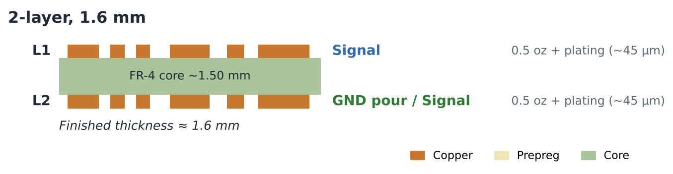
- Bottom Layer Ground Integrity: Maintain 75%+ unbroken ground copper on L2; never route long signal buses that slice the ground plane into isolated islands.
- Coplanar Waveguide (CPWG): Surround critical clock and RF traces with coplanar ground shielding stitched to the bottom reference plane.
- Local Loop Decoupling: Position decoupling capacitors directly adjacent to IC power pins, routing ground vias immediately to bottom copper without trace necking.
6. The 4-Layer Board: Standard vs. Shielded Configurations
The 4-layer stackup is the workhorse of mainstream commercial electronics. It should be the absolute minimum starting point for any design featuring fast microcontrollers, USB 2.0 High Speed (480 Mbps), 10/100 Ethernet, switching power converters, or regulatory EMC requirements (CISPR 32 / FCC Part 15 Class B).
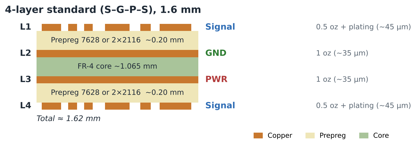
The standard industry stackup uses an S-G-P-S configuration with a thick 1.065 mm center core and thin 0.20 mm outer prepreg dielectrics. Layer 1 signals reference the L2 ground plane directly with excellent field containment. However, Layer 4 signals reference the L3 power plane. While high-frequency return currents travel smoothly along the power plane, any transition of an L4 signal to L1 forces the return current to jump between the power and ground planes through nearby decoupling capacitors. To prevent high-frequency EMI, keep L4 traces short and position a 100 nF capacitor adjacent to every layer-transition via.
For severe EMC environments, the alternative G-S-S-G shielded stackup places solid ground planes on L1 and L4, sandwiching routing on inner layers L2 and L3. While this provides superior Faraday cage containment, inner signals must be routed orthogonally to prevent broadside crosstalk, and power must be distributed as wide copper necks on signal layers.
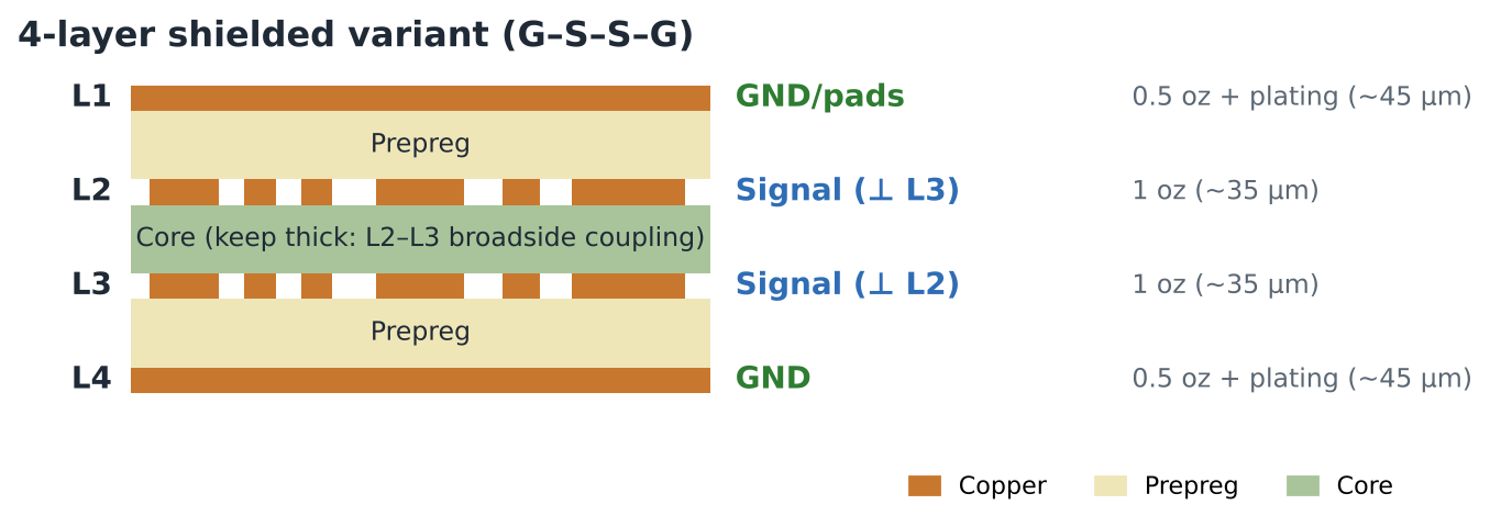
For radiated emission-critical designs, outer ground planes provide total containment. However, inner signals L2 and L3 are broadside-coupled and require orthogonal routing and thick core separation.
7. The 6-Layer Board: Configurations A, B, and C
Moving from 4 to 6 layers provides an extra pair of copper layers, enabling cleaner BGA breakout and robust power distribution. However, configuration choice is paramount. Many engineers make the disastrous mistake of selecting Configuration A (S-G-S-S-P-S) simply to maximize routing capacity.
In Configuration A, inner layers L3 and L4 run parallel to each other with no intervening ground shield, resulting in severe broadside crosstalk. Furthermore, L4 and L6 reference power, exacerbating common-mode radiation. Many designs migrating from 4 to 6 layers using Configuration A fail EMC testing worse than the 4-layer original.
The recommended industry standard is Configuration B (S-G-S-P-G-S). Every single signal layer is placed adjacent to a dedicated reference plane. L3 is an asymmetric stripline referenced primarily to L2 ground, while L4 and L5 form a tightly coupled PWR/GND plane pair separated by only 0.13 mm of prepreg, providing excellent distributed high-frequency decoupling.
For RF and sensitive mixed-signal applications, Configuration C (G-S-G-P-S-G) sacrifices routing density for maximum isolation, encasing internal routing between solid ground barriers.
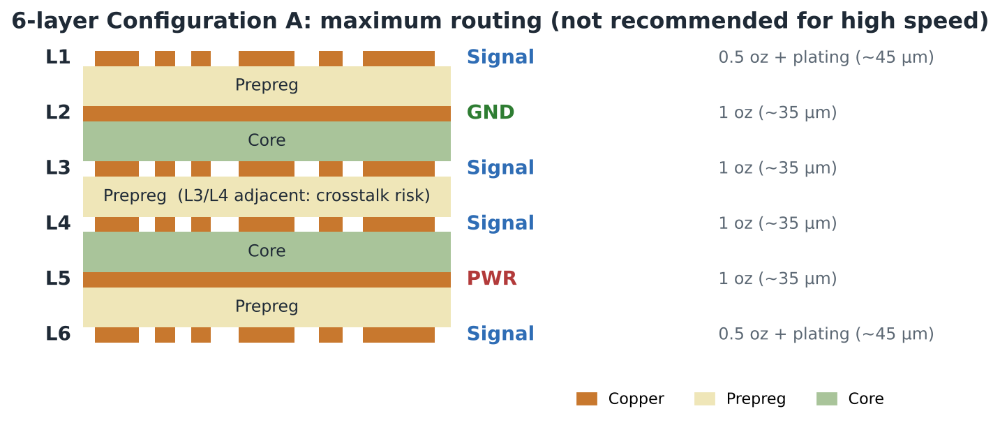
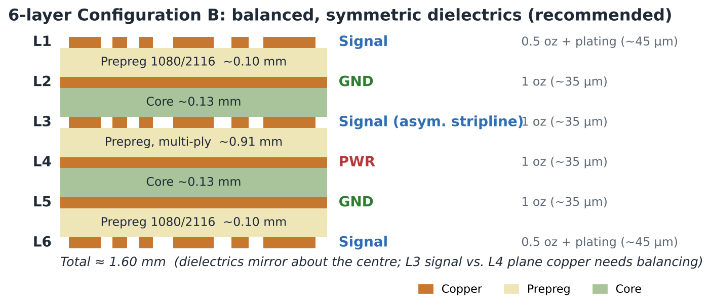
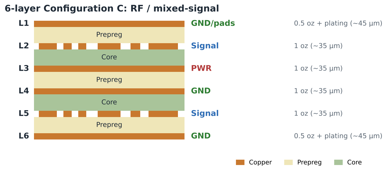
| Configuration | Layer Assignment | Signal Reference Plane | Engineering Trade-offs & Recommendation |
|---|---|---|---|
| Configuration A (Max Routing) | S1 - G2 - S3 - S4 - P5 - S6 | L3 references GND; L4 references PWR | Severe L3/L4 broadside crosstalk; DO NOT USE for high-speed digital |
| Configuration B (Balanced) | S1 - G2 - S3 - P4 - G5 - S6 | L1/L3 ref G2; L6 ref G5 | Recommended general purpose; balanced dielectrics, tightly coupled P4/G5 pair |
| Configuration C (RF / Mixed) | G1 - S2 - G3 - P4 - S5 - G6 | L2 ref G1/G3; S5 ref G6 | Maximum EMI containment and analog/digital isolation; lower routing density |
8. The 8-Layer Board: High-Speed Striplines and Dual Power Domains
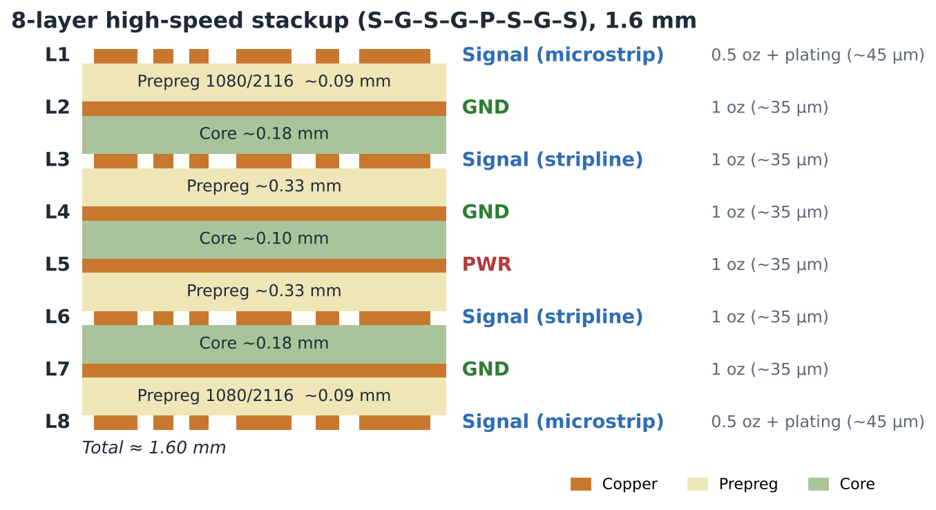
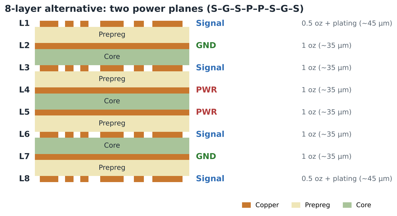
Eight layers represents the practical entry point for high-performance processors, DDR4/DDR5 memory subsystems, multi-gigabit SerDes interfaces, and complex FPGAs. An 8-layer architecture provides two fully shielded internal stripline routing layers (L3 and L6) sandwiched between solid reference planes.
In our recommended 8-layer stackup (S-G-S-G-P-S-G-S), L3 routes between L2 ground and L4 ground, providing total stripline containment with zero reference-plane bounce. L6 routes between L5 power and L7 ground, maintaining tight return paths. Crucially, layers L4 (GND) and L5 (PWR) are placed with minimal spacing (0.10 mm), creating a high-capacitance, low-inductance power distribution core.
At 8 layers and above, two critical high-speed phenomena must be managed: fiber-weave timing skew and via stub resonance. Standard coarse glass styles (like 7628) produce localized dielectric variations between glass bundles (Er = 6) and resin pockets (Er = 3). On multi-Gbps differential pairs, one trace running over glass while its pair runs over resin creates intra-pair skew that closes the receiver eye. Using spread-glass styles (1078, 3313) or routing traces at a 10-15 degree angle across the panel weave eliminates this hazard.
Additionally, through-hole via stubs act as quarter-wave resonant notch filters: fres = c / (4 x Lstub x sqrt(Er)). A 2.0 mm stub resonates near 19.5 GHz, degrading channels operating at 10-25+ Gbps. For 25+ Gbps NRZ or PAM4 links, back-drilling unused via stubs to under 0.20 mm is essential.
9. 10 to 16+ Layers and High-Density Interconnect (HDI)
When devices feature 1,000+ ball BGAs, 0.65 mm or sub-0.5 mm ball pitches, or 25-112 Gbps PAM4 SerDes channels, standard through-hole drilling physics reaches a hard mechanical limit. Traditional dog-bone fanout cannot escape interior ball rows without consuming all routing channels.
Minimum signal layers required for BGA escape can be estimated using: Nlayers approx 1 + ceil((Rtotal - 2) / r), where Rtotal is the total row depth to package center and r is the number of routable traces between via pads. At 0.8 mm pitch, r is typically 1; at 0.65 mm and below, r drops to zero, making laser-drilled microvias and High-Density Interconnect (HDI) structures unavoidable.
IPC-2226 standardizes HDI builds into Type I (1+N+1), Type II (with buried core vias), Type III (2+N+2 multi-lamination), and Any-Layer (ELIC). Each sequential build-up layer pair requires an additional lamination cycle in the press, adding 15-30% to bare-board cost and compounding dimensional registration tolerances.
Reliability alert: IPC-WP-023 documents latent failure risks at the interface of stacked microvias when subjected to multiple lead-free reflow shocks. Wherever possible, staggered microvias should be preferred over stacked microvias unless space constraints strictly require stacked via-in-pad structures.
| HDI Classification | IPC-2226 Definition | Lamination Cycles | Primary Industry Applications |
|---|---|---|---|
| Type I (1+N+1) | 1 microvia layer on each side of rigid core, through-vias | 2 cycles | 0.65-0.8 mm BGAs, compact IoT gateways, drone controllers |
| Type II | Type I with buried mechanically drilled vias in core | 2 cycles | High-density carrier boards with dense core power routing |
| Type III (2+N+2) | Two sequential microvia build-up layers per side | 3 cycles | 0.5 mm pitch mobile processors, compact aerospace electronics |
| Any-Layer (ELIC) | Every layer pair interconnected by copper-filled microvias | N/2 cycles | Flagship smartphones, wearable computers, ultra-dense compute modules |
10. What Your Stackup Does on the Assembly Line (The EMS Reality)
Most PCB stackup tutorials conclude when Gerber files are generated. But for an electronics manufacturing services (EMS) partner, that is where the real physical challenge begins. The stackup directly governs surface-mount reflow yield, thermal soldering profiles, and long-term joint integrity.
Dynamic Reflow Warpage: While IPC-6012 measures bow and twist at 20 deg C, what matters during assembly is flatness at 217-260 deg C. If an asymmetric stackup causes the PCB to smile (concave bow) while a large BGA package cries (convex bow), corner solder balls lose physical contact with solder paste deposits during the liquidus phase. This creates insidious Head-in-Pillow (HiP) and Non-Wet Open (NWO) defects that can pass basic in-circuit testing and fail later in field service.
Thermal Mass and Profiling: A 12-layer, 2.4 mm board with heavy 2 oz copper ground planes acts as an enormous heat sink. Small 0201 passives at the perimeter reach peak temperature long before the center balls of a 40x40 mm BGA. Assembly engineers must utilize multi-channel profiling thermocouples embedded directly beneath component packages, extending soak zones to ensure uniform delta-T across the assembly.
Through-Hole Barrel Fill: IPC-A-610 Class 2 and 3 require 75% vertical solder fill for plated through-hole pins. Connecting PTH pins directly to internal copper planes without thermal spoke relief sinks heat away faster than wave or selective solder nozzles can supply it, causing insufficient barrel fill.
Via-in-Pad Voiding: Placing open vias directly within BGA or QFN solder pads wicks molten solder into the hole during reflow, starving the joint and causing severe voiding. For any via-in-pad geometry, always specify IPC-4761 Type VII (filled with non-conductive epoxy and over-plated with flat copper).
| Surface Finish | Key Strengths | Critical Multilayer Assembly Watch-Outs |
|---|---|---|
| ENIG (Electroless Nickel Immersion Gold) | Planar surface, excellent for fine-pitch BGA and microvias | Black pad risk if nickel phosphorus bath chemistry is unmonitored |
| ENEPIG (Nickel / Palladium / Gold) | Zero black pad risk; wire-bondable; excellent for multi-reflow | Higher chemical process cost; used in mission-critical applications |
| Immersion Silver | Lowest insertion loss at multi-GHz frequencies; planar | Susceptible to tarnish, micro-voids, and atmospheric sulfur corrosion |
| OSP (Organic Solderability Preservative) | Economical, flat copper surface | Degrades rapidly with each heat cycle; difficult for double-sided reflow |
| HASL Lead-Free | Robust solderability, low cost | Non-planar solder mounds; causes BGA bridging and tombstones |
11. Cost Economics vs. System-Level Yield
Purchasing departments frequently resist moving from 4 to 6 layers or from 6 to 8 layers based solely on bare-board price quotes. However, evaluating PCB cost in isolation is a costly procurement fallacy.
At the bare-board level, doubling layer count from 4 to 8 layers typically increases bare-board unit cost by 1.8x to 2.4x. However, in modern electronics assemblies, the bare board rarely accounts for more than 8-12% of the total Bill of Materials (BOM) cost.
A properly planned 6-layer or 8-layer stackup routinely reduces overall product cost by shrinking overall board surface area, eliminating discrete EMI filtering chokes, removing stamped metal shielding cans, and avoiding catastrophic compliance test re-spins ($15,000 to $40,000 per chamber session plus months of market delay). More importantly, robust thermo-mechanical symmetry directly elevates surface-mount First Pass Yield (FPY).
| Layer Count Category | Relative Bare-Board Cost Index | Typical Lamination Cycles | System Cost Impact |
|---|---|---|---|
| 2-Layer Standard FR-4 | 1.0x | 1 cycle | Baseline cost; high external filtering and shielding requirements |
| 4-Layer Standard FR-4 | 1.3x - 1.8x | 1 cycle | Standard entry point; low EMC risk for general digital |
| 6-Layer Balanced FR-4 | 2.0x - 2.6x | 1 cycle | Shrinks board area 25-35%; eliminates multi-rail filtering |
| 8-Layer High-Speed FR-4 | 2.8x - 3.6x | 1 cycle | Enables DDR4/PCIe; drops failure rates under high-density BGAs |
| 10-12 Layer Enterprise | 3.6x - 4.8x | 1 cycle | Accommodates 1,000+ pin processors; ultra-low impedance PDN |
| HDI 1+N+1 to 2+N+2 | 4.5x - 7.0x+ | 2-3 cycles | Permits ultra-miniature form factors and 0.5 mm ball pitch ICs |
“The bare board represents under 10% of total BOM cost. Sacrificing layer count to save a dollar on bare laminate invariably wastes tens of thousands in EMC chamber re-spins and assembly line rework.”
12. Production Case Studies from the Line
To understand the direct connection between stackup geometry and production yield, consider three anonymized cases resolved on our manufacturing floor:
Case 1: The 4-to-6 Layer CISPR 32 Emissions Spike. An industrial IoT gateway incorporating DDR3L memory and 100 Mbps Ethernet migrated from 4 to 6 layers to ease routing congestion. The layout team adopted Configuration A (S-G-S-S-P-S). In pre-compliance radiated emissions, clock harmonics spiked 8 dB over the CISPR 32 Class B limit at 400 MHz. Analysis revealed that DDR3 data strobes on L3 and L4 were broadside-coupled, while L4 signals referenced a split power plane. Re-stacking the design to Configuration B (S-G-S-P-G-S) without changing board dimensions dropped emissions by 14 dB, delivering full regulatory compliance on the first re-test.
Case 2: 0.8 mm BGA Head-in-Pillow Fallout. An automotive telematics unit built on an asymmetric 6-layer stackup experienced a 4.2% failure rate at end-of-line functional test. X-ray inspection and micro-sectioning revealed Head-in-Pillow defects along the two outer corner rows of a 484-ball 0.8 mm FPGA. Dielectric thicknesses had not been mirrored, and L3 had only 15% copper coverage while mirror layer L4 was a solid 1 oz ground plane. Adding copper thieving to L3 and balancing core thicknesses eliminated dynamic reflow warpage, slashing BGA assembly defect rates to under 0.03% (within IPC Class 3 limits).
Case 3: CAD Default Impedance Discrepancy. A dual PCIe Gen3 carrier board routed differential pairs using CAD default nominal prepreg thicknesses. When fabricator TDR coupons were tested per IPC-TM-650 2.5.5.7, measured differential impedance was 78 Ohms against an 85 Ohm target (outside the +/- 10% budget). Recalculating trace geometries using the fabricator's true pressed thickness and high-frequency Dk restored differential impedance to 85.4 Ohms.
13. 7-Step Layer Count Selection Methodology
To ensure consistent first-pass success, every hardware development program should follow this sequential 7-step stackup decision framework:
Step 1: BGA Escape Analysis. Identify the finest-pitch, highest-pin-count BGA. Determine whether dog-bone through-vias suffice or if microvia HDI is required. Calculate minimum signal routing layers.
Step 2: Interface Inventory. List every high-speed net (DDR, USB, PCIe, Ethernet, SerDes) with its edge rate, target impedance, length matching tolerance, and required reference planes.
Step 3: PDN Analysis. Tabulate all voltage rails. Calculate target impedance for core rails: Ztarget = (Vrail x Ripple) / Delta-I. Identify rails requiring dedicated plane pairs versus wide copper pours.
Step 4: EMC & Regulatory Boundaries. Review target standards (FCC Class B, CISPR 32, CISPR 25 automotive). Designs with tight margins dictate stripline routing encased between ground planes.
Step 5: Mechanical & Enclosure Constraints. Establish finished board thickness (e.g. 1.6 mm +/- 10%). Confirm connector hole aspect ratios and press-fit pin tolerances.
Step 6: SMT Assembly Review. Review stackup with your EMS partner. Verify thermo-mechanical symmetry, thermal relief rules for PTH pins, and via-in-pad plating specifications.
Step 7: Fabricator Sign-Off. Before routing commences, obtain the fabricator's calculated stackup sheet specifying pressed prepreg plies, glass styles, and field-solved trace widths.
- BGA Escape: Minimum routing layers set by finest ball pitch.
- Interface Inventory: Edge rates dictate transmission line treatment.
- PDN Architecture: Core rails dictate plane pair capacitance.
- EMC Containment: Stripline routing for automotive and medical limits.
- Mechanical Specs: Finished thickness and drill aspect ratios.
- Assembly Review: Warpage risk assessment and thermal mass profiling.
- Fab Engagement: Pre-layout stackup sheet and field solver verification.
14. Recurring Design Errors and Mitigation Matrix
The following troubleshooting matrix outlines the twelve most prevalent stackup design errors observed on production floors, their physical consequences, and their immediate corrective engineering actions.
| Design Error | Physical Consequence on Line | Corrective Engineering Action |
|---|---|---|
| Asymmetric stackup or copper balance | Bow and twist during reflow, BGA opens, Head-in-Pillow | Mirror dielectric thicknesses, glass styles, and add copper thieving |
| Adjacent internal signal layers | Broadside crosstalk, unpredictable timing jitter | Insert ground reference plane or route strictly orthogonally |
| Traces crossing plane splits | Return path discontinuity, high loop EMI, common-mode noise | Re-route within plane boundaries or bridge with stitching capacitors |
| Layer transitions without return vias | Increased loop inductance, high-frequency ground bounce | Place GND stitching via within 1 mm of every signal transition via |
| Using CAD default dielectric values | Impedance out of tolerance by 15-30% | Base all trace widths on fabricator's pressed thickness and field solver |
| Specifying +/- 5% impedance by default | Unnecessary yield loss and cost surcharges at fabricator | Use +/- 10% standard tolerance unless SI budget strictly requires tighter |
| Coarse 7628 glass under multi-Gbps pairs | Fiber-weave intra-pair skew, differential eye closure | Specify spread-glass styles (1078, 3313) or 10-15 deg angle routing |
| Unchecked via stubs on 10+ Gbps links | Quarter-wave resonant notches, severe insertion loss | Back-drill stubs to < 0.20 mm residual length or employ blind vias |
| Standard-Tg FR-4 on thick lead-free boards | PTH barrel cracking, inner-layer delamination under reflow | Specify laminate with Tg >= 170 deg C, Td >= 340 deg C, T260 >= 30 min |
| Open via holes placed in SMT pads | Solder wicking, starving joint, excessive voiding under BGA | Specify IPC-4761 Type VII filled and copper-capped via-in-pad |
| Solid copper connections on PTH pins | Poor barrel fill (< 75%), failed IPC-A-610 inspection | Apply thermal relief spoke patterns on all plane connections |
| Omitting stackup table on fab drawing | Fabricator builds arbitrary stackup; inconsistent impedance | Include full layer stackup, material part numbers, and coupon requirements |
15. Fabrication and Assembly Documentation Checklist
A flawless stackup design is useless if it is not clearly communicated to manufacturing partners. Fabrication and assembly packages should contain explicit documentation to prevent interpretation errors.
Fabrication Drawing Essentials: Detailed layer sequence and copper weights (base and finished); exact dielectric thickness per gap with allowable tolerance; laminate specification by IPC-4101 slash sheet and manufacturer material code; required Dk/Df values at target frequency; controlled impedance coupon requirements per IPC-TM-650 2.5.5.7; drill table specifying whether dimensions indicate drilled or finished hole sizes; and via protection class per IPC-4761.
Assembly Drawing Essentials: Panel drawing with tooling holes, fiducials, break-away rail tabs, and component keep-outs (minimum 3 mm from V-score); IPC-A-610 performance class (Class 2 or Class 3); maximum allowable component thermal-pad voiding; moisture handling and bake schedules per IPC-1601; and test-point access guidelines for ICT and flying-probe verification.
- Fabrication: Explicit layer table, IPC-4101 slash sheets, impedance coupon specs, and drill tolerances.
- Assembly: Panelization drawing, fiducial markers, IPC-A-610 Class 2/3 criteria, and moisture handling.
- Quality Gates: IPC-TM-650 coupon micro-sectioning and 100% netlist flying-probe continuity testing.
16. Conclusion and Engineering Takeaways
Layer count is never an arbitrary starting point; it is the physical consequence of signal edge rates, BGA pin pitch, return-path loops, and thermal reflow mechanics. The physics of modern electronics is uncompromising: return currents follow minimum inductance, characteristic impedance depends on sub-millimeter geometry, closely spaced planes act as distributed capacitors, and asymmetric copper warps under thermal shock.
By designing the stackup first and treating thermo-mechanical balance as a non-negotiable assembly requirement, engineering teams can eliminate weeks of layout rework, avoid costly EMC chamber failures, and achieve high first-pass manufacturing yields.
Send your proposed stackup or preliminary Gerber files to Shematic's engineering desk. Our team performs automated DFM and BOM scrub in under 60 seconds, followed by comprehensive engineering review in under 2 hours, supporting prototype turnaround in under 48 hours with 99.97% First Pass Yield.
Key Takeaways
- Layer count is the analytical result of BGA escape routing, interface budgets, PDN target impedance, and EMC limits, never an arbitrary starting guess.
- The stackup architecture, not the layer count, governs electromagnetic behavior: what each trace references, dielectric heights, and cross-laminate symmetry.
- Always use the fabricator's pressed prepreg thicknesses and high-frequency Dk; relying on CAD default values is the leading cause of impedance coupon failure.
- Thermo-mechanical asymmetry that appears benign in CAD becomes severe dynamic warpage at 245-260 deg C, inducing BGA Head-in-Pillow and open joint defects.
- Bare-board cost represents under 10% of total BOM; investing in optimal layer counts eliminates costly shielding cans, filter components, and EMC re-spins.
Conclusion
Successful electronics hardware development requires harmonizing EDA design desk intentions with manufacturing line physics. By establishing rigorous stackup architectures before trace routing begins, engineering teams protect signal integrity, guarantee PDN stability, and ensure robust surface-mount assembly yield.
Whether executing high-density 0.65 mm BGA escape routing, multi-gigabit differential interfaces, or high-reliability automotive assemblies, treating stackup design as a holistic discipline bridges the concept-to-scale continuum.
Verified Sources & References
- IPC Standard SpecificationIPC-2141A: Design Guide for High-Speed Controlled Impedance Circuit BoardsIPC - Association Connecting Electronics Industries
- IPC HDI StandardIPC-2226: Sectional Design Standard for High Density Interconnect (HDI) Printed BoardsIPC - Association Connecting Electronics Industries
- IPC Acceptance StandardIPC-A-610: Acceptability of Electronic AssembliesIPC - Association Connecting Electronics Industries
- High-Temp Flatness GuidelineIPC-9641: High Temperature Printed Board Flatness GuidelineIPC - Association Connecting Electronics Industries
- Reference ArchitectureSignal and Power Integrity - SimplifiedEric Bogatin, Prentice Hall
Bring Your Hardware to Life with Shematic
Turn your schematics and BOM into functional prototypes in under 48 hours with 99.97% First Pass Yield. No legacy delays. No factory black boxes.